Driving principle of LVDS LCD
Date:2019-04-26
We have introduced the LVDS signal output interface before. We know that LVDS interface is the general interface standard of LCD panel, which is mostly used on the display screen with the size of more than 7 inches. Today we will explain the driving principle of LVDS LCD screen
Overview of LVDS output interface
In addition to RGB data signal, the digital signal output from LCD driver board also includes row synchronization, field synchronization, pixel clock and so on. The maximum frequency of pixel clock signal can exceed 28MHz. Using TTL interface, the data transmission rate is not high, the transmission distance is short, and the anti electromagnetic interference (EMI) ability is poor, which will have a certain impact on RGB data; In addition, the TTL multi-channel data signal is transmitted by the way of wire arrangement, and the number of the whole wire arrangement reaches dozens of channels, which is not only inconvenient to connect, but also not suitable for the trend of ultra-thin. By using LVDS output interface to transmit data, these problems can be solved easily, and data transmission with high speed, low noise, long distance and high accuracy can be realized.
Signal driving principle of LVDS interface (1920 * 1080)
1、 The relationship between clock and pixel
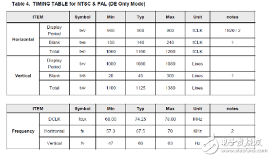
One field: 60hz-16.667ms, 1125 lines (1080 lines valid)
——Refresh pixels: 1920 * 1080 / vertical
One line: 67.5khz-14.815us, (= 60Hz * 1125), 1100 * 2 points (1920 points = 960 * 2 points valid)
——Refresh pixels: 1920 / horizontal
Clock:74.25MHz-13.468ns,(=67.5KHz*1100)
——Refresh pixels: 2 / clock
For the above, please refer to Appendix A: signal timing characteristics of screen specification.
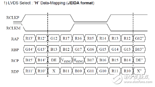
2、 LVDS signal transmission rules
Taking the double 8-bit signal interface as an example, each clock (odd + even) and LVDS interface has 4 * 2 pairs of differential pairs (double 8-bit) transmitting at the same time, and each 4 pairs of differential pairs is responsible for 1 pixel; Each clock (odd + even) transmits 2 pixels;
Every 4 differenti
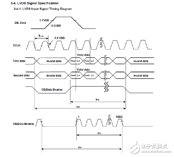
Appendix B: LVDS signal timing
Appendix C: screen specification data transmission format