Difference between TTL signal interface and CMOS level signal interface
Date:2019-04-26
The difference between TTL and CMOS level
When we select small and medium-sized LCD, we often see many LCD signal interfaces write TTL, some write this CMOS interface, common CMOS interface Mitsubishi LCD, and whether we know the relationship and difference. Let's explain it below.
1、 TTL
The main type of TTL integrated circuit is transistor transistor logic gate, and most of TTL uses 5V power supply
1. output high level uoh and output low level uoluoh ≥ 2.4V, UOL ≤ 0.4V
2. input high level and input low level UIH ≥ 2.0V, UI ≤ 0.8V
2、 CMOS
CMOS circuit is a voltage control device, with great input resistance and is very sensitive to interference signal. Therefore, the input end not used should not open circuit. The advantages of CMOS circuit are wide noise tolerance and small static power consumption
1. output high level uoh and output low level uoluoh ≈ VCC, UOL ≈ GND
2. input high-level uoh and input low-level uoluih ≥ 0.7vcc, UIL ≤ 0.2vcc (VCC is power voltage, GND is ground)
From the above, we can see that:
In the same 5V power supply voltage, COMS circuit can directly drive TTL, because the output high level of CMOS is greater than 2.0V and the output low level is less than 0.8V; However, TTL circuit can not drive CMOS circuit directly. If TTL output high level is greater than 2.4V, if it falls between 2.4V and 3.5V, CMOS circuit can not detect high level and low level is less than 0.4V to meet the requirements. Therefore, pull resistance should be added when TTL circuit drives COMS circuit. If different voltage power supply occurs, it can also be judged by the above method
If there is a 3.3V COMS circuit in the circuit to drive 5V CMOS circuit, such as 3.3V single chip microcomputer to drive 74hc, there are several ways to solve this problem. The simplest is to directly change 74hc into a chip of 74HCT (74 series input and output are described below), because 3.3V CMOS can directly drive 5V TTL circuit; Or voltage conversion chip; In addition, the i/o port of the MCU is set as open leakage, and then the pull resistance is added to 5V. In this case, the resistance size must be adjusted according to the actual situation to ensure the rising time of the signal
3、 74 series introduction
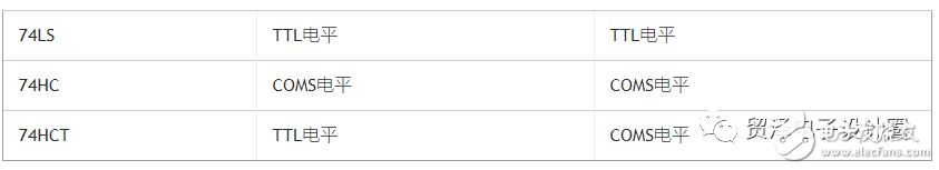
Series 74 can be said to be the most frequently contacted chips. 74 series is divided into many kinds. The most commonly used chips are as follows: 74LS, 74hc and 74HCT. The differences in level of these three series are as follows:
TTL and CMOS levels
1. TTL level (what is TTL level)
Output high level > 2.4V, output low level = 2.0V, input low level VIH, input low level VIH > VT > VIL > Vol
6: IOH: the output of logic gate is load current at high level (pull current). 7: IOL: the output of logic gate is load current at low level (pour current). 8: IIH: the input of logic gate is current at high level (pour current). 9: Il: the input of logic gate is current at low level (pull current)
The output of the gate circuit is directly led out as the output terminal without the load resistance in the integrated unit. This form of gate is called the open gate. The open TTL, CMOS and ECL gates are called open collector (OC), open drain (OD) and open emitter (OE) respectively. Whether to connect the pull-up resistance (OC, OD gate) or pull-down resistance (OE gate) should be checked when using, For open collector (OC) gate, the pull-up resistance RL should meet the following conditions:
(1):RL < (VCC-Voh)/(n*Ioh+m*Iih)(2):RL > (VCC-Vol)/(Iol+m*Iil)
Where N: the number of open gates of line and; m: The number of inputs to be driven
10: Common logic level
·Logic level: TTL, CMOS, LVTTL, ECL, PECL, GTL; RS232, RS422, LVDS, etc
·According to the typical voltage, TTL and CMOS logic levels can be divided into four categories: 5V series (5V TTL and 5V CMOS), 3.3V series, 2.5V series and 1.8V series
·5V TTL and 5V CMOS logic levels are common logic levels
·3 V and below logic level is called low voltage logic level, commonly used as LVTTL level
·There are 2.5V and 1.8V logic levels for low voltage
·ECL / PECL and LVDS are differential input and output
·RS-422 / 485 and RS-232 are serial interface standards, RS-422 / 485 is differential input and output, RS-232 is single ended input and output. OC gate, also known as collector open (drain open) NAND gate circuit, open collector (open drain)
Why introduce OC gate?
In practical use, sometimes two or more NAND gates need to be connected to the same wire to transmit the data (state level) on these NAND gates with the same wire. Therefore, a new NAND gate circuit OC gate is needed to realize "line and logic"
1. Because the collector of the output tube of the OC gate circuit is suspended, a pull-up resistor RP should be connected to the power supply VCC. The OC gate uses the pull-up resistor to output high level. In addition, in order to increase the driving ability of the output pin, the selection principle of the pull-up resistor value should be large enough considering the power consumption reduction and the chip's current pouring ability; It should be small enough to ensure enough driving current
2. In practical applications such as bus transmission, the output terminals of multiple gates need to be connected in parallel. However, the output terminals of TTL gates can not be directly connected in parallel, otherwise the output tubes of these gates will form a large short-circuit current (pouring current) due to low impedance, In hardware, it can be realized by OC gate or three state gate (st gate). When using OC gate to realize line and line connection, a pull-up resistor should be added at the output port at the same time
3. The three state gate (st gate) is mainly used to share the data bus with multiple gate outputs. In order to avoid multiple gate outputs occupying the data bus at the same time, only one of the enable signals (EN) of these gates is allowed to be an effective level (such as a high level). Because the output of the three state gate is a push-pull low resistance output and does not need to be connected with a pull-up (load) resistor, the switching speed of the three state gate is faster than that of the OC gate, Three state gates are often used as output buffers. What are OC and OD?
Open collector gate (open collector oC or open drain OD)
Open drain means open drain output, which is equivalent to open collector output, that is, open collector output in TTL. It is generally used for line or, line and, or current drive
Open drain is for MOS and open collector is for bipolar. There is no difference in usage
a. Using the drive ability of external circuit, reduce the internal drive of IC. Or drive the load higher than the chip power supply voltage. B. multiple open drain output pins can be connected to a line. Through a pull-up resistor, the "and logic" relationship can be formed without adding any devices. This is also I2C, If it is used as a totem output, it must be connected with pull-up resistor. When it is connected with capacitive load, the drop delay is the transistor in the chip, which is an active drive, and the speed is faster; The rising delay is a passive external resistor, which is slow. If the speed is high, the resistance selection should be small, and the power consumption will be large. So the load resistance selection should consider both power consumption and speed. C. the transmission level can be changed by changing the voltage of the pull-up power supply. For example, the TTL / CMOS level output can be provided by adding the pull-up resistance. D. the open drain pin does not connect the external pull-up resistance, Generally speaking, open drain is used to connect devices with different levels and match them
The normal CMOS output stage is the upper and lower tubes. If the upper tube is removed, it is open-drain. There are two main purposes of this output: level conversion and line to line connection
Because the drain stage is open, the back stage circuit must be connected with a pull-up resistor. The supply voltage of the pull-up resistor can determine the output level. In this way, you can convert any level
Line and function are mainly used in the situation where multiple circuits pull down the same signal. If the circuit does not want to pull down, it will output high level. Because the tube on the open-drain is removed, the high level is realized by the external pull-up resistor. (in normal CMOS output stage, if one output is high and the other is low, it is equal to power short circuit.)
Open-drain provides a flexible output mode, but it also has its weakness, that is, it brings the rising edge delay. Because the rising edge charges the load through the external pull-up passive resistor, when the resistor is selected small, the delay is small, but the power consumption is large; If the delay is required, the falling edge output is recommended.
Hangzhou Xuhong Technology Co., Ltd. is a technology-based company of industrial color LCD module, industrial control display products and touch screen control. It is a professional supplier of industrial LCD drive solutions. It is an enterprise unit that carries out display and touch control of terminal equipment through LCD products and display drive solutions. Our long-term stable supply of 3.5 "- 32" industrial LCD screen, TFT LCD screen brand diversification, complete models, can meet different customers under different application environments, medical, vehicle special industry wide temperature, bright, wide angle Industrial LCD screen all stable supply.