How to solve the electromagnetic interference of the projection capacitance touc
Date:2019-04-26
Nowadays, the projected capacitive touch screen, which is widely used in portable devices, is vulnerable to electromagnetic interference. The interference voltage from inside or outside will be coupled to the touch screen device through capacitance. These interference voltages will cause the charge movement in the touch screen, which may confuse the measurement of the charge movement when the finger touches the screen. Therefore, the effective design and optimization of the touch screen system depends on the understanding of the interference coupling path, as well as its reduction or compensation as far as possible.
The interference coupling path involves parasitic effects, such as transformer winding capacitance and finger device capacitance. The source and size of interference can be fully recognized by modeling these influences properly.
For many portable devices, battery charger is the main interference source of touch screen. When the operator's fingers touch the touch screen, the capacitance generated makes the interference coupling circuit of the charger close. The quality of internal shielding design and proper grounding design are the key factors affecting the interference coupling of charger.
The projected capacitive touch screen can accurately locate the position where the finger touches the screen. It can determine the position of the finger by measuring the tiny change of the capacitance. In this kind of touch screen application, a key design problem to be considered is the influence of electromagnetic interference (EMI) on the system performance. Performance degradation caused by interference may have an adverse impact on touch screen design.
Structure of projection capacitive touch screen
A typical projected capacitive sensor is mounted under a glass or plastic cover. Figure 1 shows a simplified side view of a two-layer sensor. The TX and Rx electrodes are connected to transparent indium tin oxide (ITO) to form a cross matrix. Each TX RX node has a characteristic capacitance. TX ITO is located
Figure 1: sensor structure reference
Working principle of sensor
Let's not consider the interference factors, to analyze the work of the touch screen: the operator's finger is at the nominal ground potential. Rx is held at ground potential through the touch screen controller circuit, while TX voltage is variable. The changing TX voltage causes the current to pass through the TX RX capacitor. A carefully balanced RX IC isolates and measures the charge entering Rx, which represents the "mutual capacitance" connecting TX and Rx.
Sensor status: not touched
Figure 2 shows a schematic diagram of the magnetic lines of force in the untouched state. In the case of no finger touch, the TX RX magnetic lines occupy a considerable space in the cover plate. The edge magnetic lines of force project beyond the electrode structure, hence the term "projected capacitance".
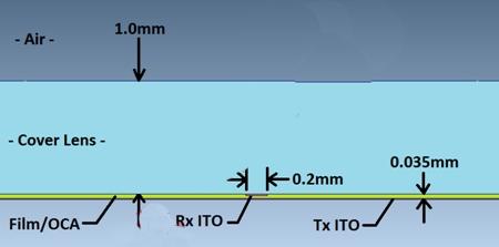
Figure 2: magnetic lines of force in untouched state
Sensor status: touch
When the finger touches the cover plate, magnetic lines of force are formed between TX and the finger, which replace a large number of TX RX edge magnetic fields, as shown in Figure 3. In this way, finger touch reduces the TX RX mutual capacitance. The charge measurement circuit recognizes the changing capacitance (△ C) and detects the finger above the TX RX node. By measuring △ C of all the intersection points of TX RX matrix, the touch distribution map of the whole panel can be obtained.
Figure 3 also shows another important effect: the capacitive coupling between the finger and the RX electrode. Through this path, electrical interference may be coupled to Rx. Some degree of finger RX coupling is inevitable.
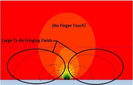
Figure 3: magnetic lines of force in touch state
Special terms
The interference of the projected capacitive touch screen is generated by the imperceptible parasitic path coupling. The term "Earth" is often used to refer to both the reference node of a DC circuit and the low impedance connection to earth: they are not the same term. In fact, for portable touch screen devices, this difference is the root cause of touch coupling interference. To clarify and avoid confusion, we use the following terms to evaluate touch screen interference.
· earth: connected to the earth, for example, through the ground wire of a 3-hole AC power outlet.
Distributed earth: capacitive connection between object and earth.
DC ground: DC reference node of portable device.
· DC power: battery voltage of portable devices. Or a charger output voltage connected to a portable device, such as the 5V VBUS in a USB interface charger.
· DC VCC (DC VCC power supply): stable voltage to power portable device electronics (including LCD and touch screen controller).
· neutral: AC power circuit (nominal at ground potential).
Hot: AC power supply voltage, applying electric energy to the zero line.
LCD VCOM coupled to touch screen receiving line
The portable device touch screen can be directly installed on the LCD display. In a typical LCD architecture, the liquid crystal material is biased by transparent upper and lower electrodes. A plurality of electrodes below determine a plurality of single pixels of the display screen; The upper common electrode is a continuous plane covering the entire visual front end of the display screen, which is biased at the voltage VCOM. In typical low-voltage portable devices (such as mobile phones), AC VCOM voltage is a square wave oscillating back and forth between DC ground and 3.3V. AC VCOM level is usually switched once per display line, so the AC VCOM frequency generated is 1 / 2 of the product of display frame refresh rate and number of lines. The AC VCOM frequency of a typical portable device may be 15 kH
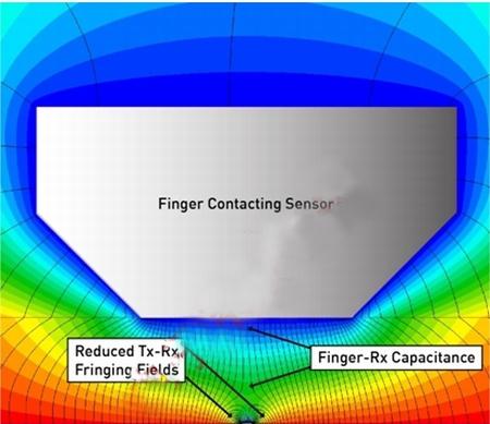
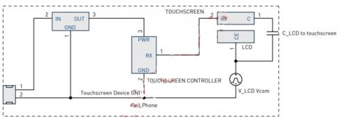
Figure 4: LCD VCOM interference coupling model
The dual touch screen consists of separate ITO layers covered with TX and Rx arrays, separated by dielectric layers. The TX lines occupy the entire width of the TX array spacing, and the lines are separated only by the minimum spacing required for manufacturing. This architecture is called self shielded because TX array shields RX array from LCD VCOM. However, through the gap between the TX bands, coupling can still occur.
In order to reduce the cost of architecture and obtain better transparency, the single touch screen installs TX and Rx arrays on a single ITO layer, and bridges each array in turn through a separate bridge. Therefore, the TX array cannot form a shielding layer between the LCD VCOM plane and the sensor RX electrode. This may cause serious VCOM interference coupling.
Charger interference
Another potential source of touch screen interference is the switching power supply of mobile phone charger powered by power supply. The interference is coupled to the touch screen by fingers, as shown in Figure 5. Small cell phone chargers usually have AC power hot line and zero line input, but no ground connection. The charger is securely isolated, so there is no DC connection between the power input and the charger secondary coil. However, this will still produce capacitive coupling through the switching power supply isolation transformer. Charger interference forms a return path by touching the screen with a finger.
Note: in this case, charger interference refers to the applied voltage of the equipment relative to the ground. This kind of interference may be described as "common mode" interference because it is equivalent to DC power supply and DC ground. If the power switch noise generated between the DC power supply and the DC ground of the charger is not fully filtered out, the normal operation of the touch screen may be affected. This PSRR problem is another problem, which is not discussed in this paper.
Charger coupling impedance
The switching interference of the charger is generated by the leakage capacitance (about 20pF) coupling between the primary and secondary windings of the transformer. This kind of weak capacitance coupling can be compensated by the parasitic shunt capacitance in the relatively distributed ground of the charger cable and the receiving equipment itself. When the device is picked up, the shunt capacitance will increase, which is usually enough to eliminate the charger switch interference and avoid interference affecting touch operation. When the portable device is connected to the charger and placed on the desktop, and the operator's fingers only touch the touch screen, there will be a worst-case interference generated by the charger.
Interference component of charger switch
Typical mobile phone charger uses flyback circuit topology. The interference waveform generated by this charger is complex and varies greatly with different chargers. It depends on the circuit details and output voltage control strategy. The amplitude of the disturbance also varies greatly, depending on the design effort and unit cost invested by the manufacturer in the shielding of the switching transformer. Typical parameters include:
Waveform: including complex pulse width modulation square wave and LC ringing waveform. Frequency: 40 ~ 150kHz under the rated load, when the load is very light, the pulse frequency or cycle hopping operation drops below 2KHz. Voltage: up to half of the peak voltage of the power supply = VRMs / √ 2.
Interference component of charger power supply
At the front end of the charger, the AC power supply voltage is rectified to generate the high voltage rail of the charger. In this way, the switching voltage component of the charger is superimposed on a sine wave half of the supply voltage. Similar to switching interference, the power supply voltage is also coupled by switching isolation transformer. At 50 Hz or 60 Hz, the frequency of this component is much lower than the switching frequency, so its effective coupling impedance is correspondingly higher. The severity of power supply voltage interference depends on the characteristics of parallel impedance to ground and the sensitivity of touch screen controller to low frequency.
Hangzhou Xuhong Technology Co., Ltd. is a technology-based company of industrial color LCD module, industrial control display products and touch screen control. It is a professional supplier of industrial LCD drive solutions. It is an enterprise unit that carries out display and touch control of terminal equipment through LCD products and display drive solutions. Our long-term stable supply of 3.5 "- 32" industrial LCD screen, TFT LCD screen brand diversification, complete models, can meet different customers under different application environments, medical, vehicle special industry wide temperature, bright, wide angle Industrial LCD screen all stable supply.